Nintendo's 8-bit console: a 6502-based CPU with built-in sound, a tile-and-sprite picture processor, and cartridges that could add hardware of their own.
Nintendo · 1983 (Japan, as the Family Computer), 1985 (North America), 1986 (Europe)
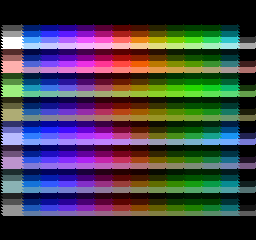
full_palette shows all 512 of the NES's colours, its 64 hues under each of the eight colour-emphasis settings, by changing the palette as the picture is drawn: the frame drawn by retro-silicon's NES, captured through its test shell. retro-silicon on the Tang Nano 20K; test ROM by blargg, CC BY 4.0.
Overview
The Nintendo Entertainment System is the console that retro-silicon builds first. It came out in Japan in July 1983 as the Family Computer, or Famicom, and reached North America in October 1985 and Europe in September 1986 [6]. By Nintendo’s count, the Famicom and NES together sold 61.91 million units worldwide [7].
Its design is small enough to understand completely. A single chip holds the processor and the sound hardware; a second chip draws the picture; and each game cartridge brings its own memory, and often extra chips that extend what the console can address. Many games relied on that last part: mapper chips in the cartridge gave them more memory, and sometimes features, than the console had on its own.
That makes it a good first system for a library of reusable parts. Its CPU is a 6502, the same family used in the Atari 2600, the Apple II and the Commodore 64, so the core built for the NES is meant to carry over to the systems that follow.
History
The Famicom was designed at Nintendo’s hardware division, Research and Development 2, led by Masayuki Uemura, who had joined Nintendo from Sharp in 1971 [9]. It launched in Japan on 15 July 1983 [6]. Nintendo’s own company history records the launch as that of the Family Computer, “known as Nintendo Entertainment System outside Japan” [8].
For the American release Nintendo reworked the console’s look and connections. The NES takes two detachable controllers, where the Famicom’s are wired in; on the Famicom the second controller has no Select or Start button but a microphone instead [5]. It also carried a lockout chip, the CIC, whose program (10NES) checks for a matching chip in the cartridge before a game can run [6]. The NES launched in North America on 18 October 1985 and in Europe on 1 September 1986 [6]. Nintendo began selling Super Mario Bros. in 1985 [8].
In Japan the Famicom was extended with the Famicom Disk System, a drive that read Nintendo’s Disk Cards, based on Mitsumi’s Quick Disk, through a RAM adapter that plugged into the cartridge slot and added RAM and an extra sound channel [10].
Specifications
CPU
Ricoh RP2A03 (NTSC) or RP2A07 (PAL): a 6502 core without the MOS 6502’s decimal mode, at 1.789773 MHz (NTSC) or 1.662607 MHz (PAL), from a 21.477272 MHz or 26.601712 MHz master clock [1][2]
Memory
2 KB of work RAM and 2 KB of video RAM, which holds the nametables [6]; 256 bytes of sprite memory (OAM) inside the picture processor [3]; 32 bytes of palette memory [4]
Video
Ricoh 2C02 (NTSC) or 2C07 (PAL) picture processor; 256 × 240 pixels [6]; a dot every 4 master clocks on NTSC (5.369318 MHz), 341 dots a line, 60.0988 frames a second on NTSC and 50.0070 on PAL [1]; a 64-entry master palette, with four background and four sprite palettes of four colours each, which allows 25 colours at once (a backdrop plus three per palette) [4]; 64 sprites, 8 × 8 or 8 × 16, at most eight on a line [3]
Audio
In the CPU chip: two pulse channels, a triangle channel, a noise channel and a delta-modulation channel (DMC) that plays 1-bit delta samples from memory [2][11]
Media
Cartridges, holding the program (PRG ROM) and the tile graphics (CHR ROM or RAM), often with a mapper chip that switches banks to reach more memory [6]; in Japan, Disk Cards through the Famicom Disk System [10]
I/O
Two controllers read one button at a time through serial shift registers, at $4016 and $4017 [5]; a lockout chip on the NES [6]
Colours on screen: the 25 is a count from the palette layout described by the NESdev Wiki [4], not a figure it states; tricks such as changing palettes mid-frame can show more.
Inside the hardware
The NES has two main chips and a cartridge that does as much as either.
The NES's two buses. The cartridge sits on both, which is how a mapper can change what the CPU and the PPU see.
How retro-silicon builds it
Boards. The NES runs on the Sipeed Tang Nano 20K, with its program ROM in the board’s SDRAM and its picture on HDMI at 720p; on the Sipeed Tang Console 138K, with its memory in block RAM; and on the TUL PYNQ-Z2, built with the open-source openXC7 toolchain, also with HDMI. See Boards.
Reference.MesenCE, an accurate open-source NES emulator, is the reference. The PPU follows MesenCE’s timing, so a frame from the core can be compared with MesenCE’s pixel for pixel, as a CRC-32 of the frame’s raw palette values.
Tests. The CPU is checked in lockstep with perfect6502, a transistor-level simulation of the original chip, and against nestest’s reference log, cycle for cycle. The system runs community test ROMs, from blargg’s PPU and timing tests to sprite hit and overflow tests, and each one’s chosen frame must give MesenCE’s CRC, in the simulation and on every board. Save states are checked by saving partway through a test, restoring, and finishing with the same CRCs as an uninterrupted run, including after moving the state from one board to another.
Firmware. The NES needs none: unlike later consoles it has no boot ROM. The cartridge’s program starts from the CPU’s reset vector.
Status
In progress: 15 of 20 parts verified on a board.
Generated from retro-silicon ac84cec; never written by hand.
The NES runs on an AMD Zynq-7020, on a TUL PYNQ-Z2, built entirely with the open-source openXC7 toolchain, and every test gives the Tang boards’ CRCs: nestest, the save-state round trip, all 42 PPU test ROMs, and HDMI at 720p, checked by checksum and through the capture device. The parts it shares with the Tang boards now count as Portable: verified on two FPGA families.
Getting there turned up four limits of the toolchain, each worked around in the board’s own files or in a part that now avoids it on every board: clock settings with fractions came out wrong, the ninth bit of a 9-bit-wide block RAM was lost, deep memories built from cascaded block RAM couldn’t be placed, and the timing varied widely from one placement to the next.
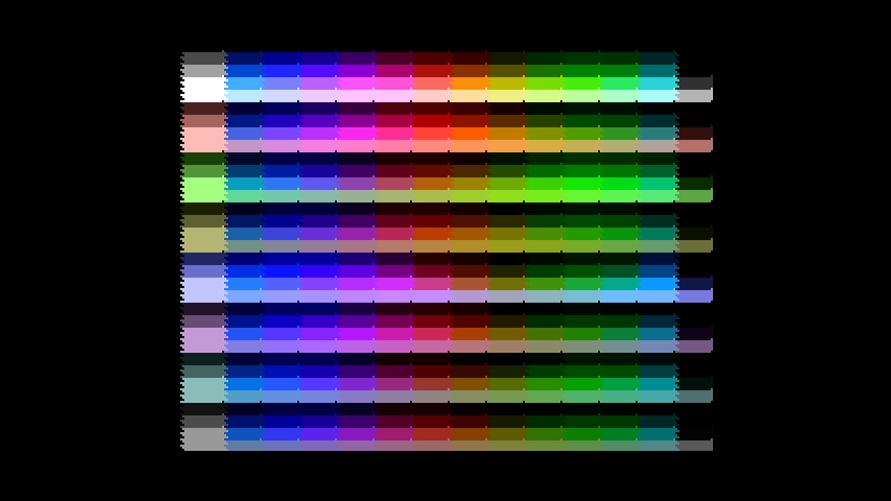
full_palette at 720p over HDMI from the PYNQ-Z2, grabbed by a USB capture device: the frame the check compares, pixel for pixel, with the one the console drew. retro-silicon on the TUL PYNQ-Z2, captured over HDMI; test ROM by blargg, CC BY 4.0.
The NES’s picture now goes out over HDMI at 720p: three times its size, centred, with the console kept in step with the display so each display frame shows one NES frame whole. On the Tang Nano 20K a checksum of every symbol sent to the display matches the simulation’s, a desk monitor shows the picture, and a USB capture device’s picture of each test’s frame matches the frame the console drew.
The board found three problems the simulation couldn’t see, all in how the open toolchain built the design rather than in the design itself, and each has a fix in place.
The NES now runs on a second board, the Sipeed Tang Console 138K, with its memory in block RAM, and every test gives the same CRCs as on the Tang Nano 20K: nestest 0xebba51ce, and all 42 PPU test ROMs with MesenCE’s frames.
A save-state controller stops the system at a frame boundary and copies the CPU, the PPU and every RAM, 20,920 bytes, out through the test shell and back. Saved partway through a test, reset, restored and finished, a run ends with the same frame, line CRCs, bus trace and cycle count as an uninterrupted one. A state saved halfway on either board also finishes on the other with MesenCE’s frames, for nmi_sync, sprite_overflow-3 and ppu_vbl_nmi-10.
The picture processor, video/ppu-2c02, draws its first frames on the board, and they match the reference emulator exactly. Its timing follows MesenCE’s, so a frame from the core and a frame from MesenCE can be compared as raw palette values, CRC for CRC.
42 test ROMs pass that way, in the simulation and on the Tang Nano 20K: blargg’s VBL and NMI tests, PPU open bus and OAM reads, the sprite hit and overflow tests, VBL/NMI timing, palette RAM, nmi_sync and full_palette. A whole frame captured from the board line by line matches MesenCE’s pixel for pixel. Five bugs planted in the PPU on purpose were each caught by the ROMs.
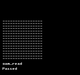
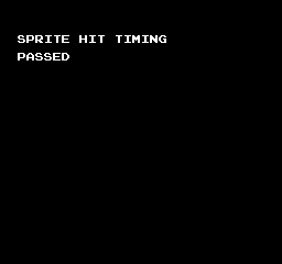
blargg's oam_read test, which reads sprite memory back through the PPU, passing: the frame drawn by retro-silicon's NES and captured line by line through its test shell. retro-silicon on the Tang Nano 20K; test ROM by blargg, CC BY 4.0.The sprite-0 hit timing test passing: the frame drawn by retro-silicon's NES, captured through its test shell. retro-silicon on the Tang Nano 20K; test ROM by blargg, CC BY 4.0.
The NES’s CPU core, cpu/6502, matches the original chip on every bus access. In simulation it ran in lockstep with perfect6502, a transistor-level model of the real 6502, over two million cycles of random code with random interrupts, and on 1,500 decimal-mode cases. All 8,991 lines of nestest’s reference log match, cycle counts included, and blargg’s test of every official opcode passes.
The lockstep also turned up three things outside our own code: a memory bug in perfect6502’s newest version, an operation perfect6502 leaves out of three rarely used opcodes, and the exact half-cycle at which the chip samples its interrupt lines.
The CPU now runs on real hardware. On the Sipeed Tang Nano 20K, systems/nes reads its program from the board’s SDRAM through the new memory/sdram controller, and nestest’s run gives the bus-trace CRC 0xebba51ce: a checksum of every bus cycle, the same in the simulation, on the board, and from the CPU’s own test bench.
The SDRAM controller worked on the board the first time: 8 MB of random data written and read back with the simulation’s CRC. The simulation had caught two of its bugs first.